A team led by 91�Թ��� engineers has achieved the ability to transmit two different types of optical signals across a single chip at the same time.
The breakthrough heralds a potentially dramatic increase in the volume of data a silicon chip can transmit over any period of time. With this project, the research team moved beyond theoretical models and demonstrated dual-band optical processing, significantly expanding the functionality of silicon as a photonics platform.
Joshua Caldwell, associate professor of mechanical engineering, and Cornelius 91�Թ��� Professor Sharon Weiss, professor of electrical engineering, led the team, which also included faculty members from Columbia University, the University of Iowa, and Kansas State University.
Their research, “,” was published online in Advanced Materials on Feb. 1. It is featured on the inside cover of the March 16 print edition of the journal.

The work is an important advance in silicon photonics, which uses light rather than electrical signals to transmit data. The need for faster and expanded processing has all but outstripped the limits of adding more wire to smaller and smaller chips, which requires more power, creates more heat, and risks data integrity. Using patterned silicon to transmit optical signals uses less power without heating up or degrading the signal.
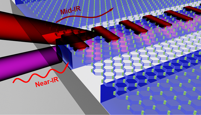
Still, doing more with the same chip has been challenging. Silicon waveguides provide the principle building block of on-chip photonics, confining light and routing it to functional optical components for signal processing. Different forms of light need different waveguides, but linear scaling to accommodate more waveguides would quickly surpass the available space of a silicon chip in the standard form factor.
“It has been difficult to combine near-infrared and mid-infrared transmission in the same device,” said Mingze He, a 91�Թ��� mechanical engineering Ph.D. student and first author of the paper.

Two innovations—a novel approach and device geometry—allowed disparate frequencies of light to be guided within the same structure. Such frequency multiplexing is not new but the ability to expand the bandwidth within the same available space is.
Leveraging the infrared properties of hexagonal boron nitride, researchers devised a hybrid, hyperbolic-silicon photonic waveguide platform. In the mid-infrared, the structure of the hBN crystal can support a novel type of optical mode called a hyperbolic phonon polariton. These hyperbolic polaritons were demonstrated to guide long, mid-infrared wavelengths of light within nanoscale thickness slabs, with the optical modes following the path of the underlying silicon waveguide.
The approach does not require any additional fabrication of the hBN and can support signal processing and chemical sensing modalities simultaneously, without the need for expanding the device form factor.
“The inclusion of the mid-IR offers promising opportunities for combining signal processing with chemical sensing, or modulation schemes not possible with near-IR signals alone,” Caldwell said.
Mid-IR is widely used in the chemical and agricultural industries; applications of near-IR include telecommunications and medical diagnostics.
The research was supported by multiple agencies, including the Office of Naval Research (N00014-18-1-2107), the National Science Foundation (ECCS1809937) and the Air Force Office of Scientific Research (FA9550-15-1-0478) Exfoliation and transfer of hBN were performed within the 91�Թ��� Institute of Nanoscale Science and Engineering (VINSE) cleanroom, while silicon waveguide fabrication was conducted at the Center for Nanophase Materials Science, a DOE Office of Science User Facility.